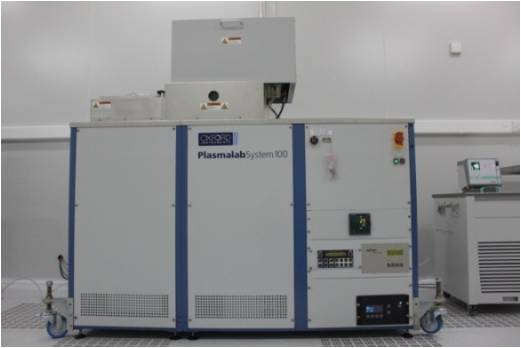
型 号:Plasmalab System 100 ICP180
功 能:
-
纳米硅刻蚀、深硅刻蚀、低温工艺、SOI工艺、SiO2刻蚀
Si etching, Nano- Si etching, Deep Si etching, SOI etching, SiO2 etching
-
刻蚀特征尺寸微米至百纳米;刻蚀深宽比可达10﹕1
Micrometersdown to hundred nanometers; Depth to width ratio up to 10﹕1
主要配置:
-
载片(Wafers):直径100mm、50mm及小碎片 (up to 100 mm wafers)
-
六路气体 (Gas lines):C4F8、SF6、CHF3、Ar、O2、PN2
-
射频源(Sources):
ICP源:3KW,13.56MHz (ICP180 power: 3kW, 13.56MHz);
RF源:600W,13.56MHz (ICP RF power: 600W, 13.56MHz);
LF脉冲源:300W,350~ 460 KHz (SOI power300W, 350 ~460 KHz)
-
下电极(Lowerelectrode):直径240mm氦气背冷辅助冷却 (240mm with backside helium cooling)
-
载片台温度范围(Temperature range):
冷却液工艺- 30℃~ 80℃ (HTR /Chiller : - 30℃~ 80℃ );
液氮低温/加热工艺- 150℃~ 400℃ (Liquid nitrogen cryo-cooled / heated process: -150℃~ 400℃ )
技术特点: